
2027 Advanced Packaging Roadmap: From 3D SoIC to Co-Packaged Optics
The 2027 advanced packaging roadmap is shaping up to be less about a single breakthrough and more about a sequence of tightly linked transitions. On one end sits 3D SoIC, a powerful expression of vertical integration that pushes logic and memory closer together than traditional packaging ever could. On the other end sits co-packaged optics, or CPO, which aims to move the bottleneck of data movement out of electrical interconnect and into the optical domain. Between them lies the broader world of advanced packaging and heterogeneous integration, where chiplets, HBM, hybrid bonding, fan-out, and new substrate technologies are converging into a new system architecture playbook.
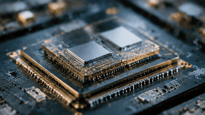
What makes 2027 interesting is not just that these technologies exist. It is that they are beginning to form a roadmap. The industry is moving from isolated demonstrations and premium applications toward more structured adoption paths. That does not mean everything will commercialize at once. It means the packaging ecosystem is now mature enough to define where each technology fits, what problem it solves, and what trade-off it demands. In that sense, the roadmap is becoming as important as the technology itself.
Why Roadmaps Matter Now
In the past, semiconductor roadmaps focused mainly on transistor scaling. Today, the center of gravity has shifted toward system integration. The reason is simple: performance growth increasingly depends on how well dies are connected, cooled, and packaged, not just how small they are. This is especially true for AI, HPC, networking, and cloud infrastructure, where bandwidth, latency, and power efficiency are often limited by package-level constraints rather than core logic itself.
A roadmap matters because it gives the industry a way to sequence technologies rather than treat them as competing abstractions. 3D SoIC is not trying to solve the same problem as CPO, and CPO is not trying to replace chiplet stacking. The real challenge is to decide when to use each, how they connect, and how they can be scaled economically. That is what the 2027 roadmap is beginning to clarify.
The Role of 3D SoIC
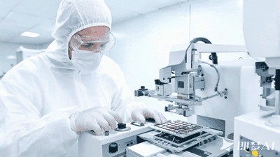
3D SoIC, or system on integrated chips, represents one of the most advanced forms of vertical heterogeneous integration. It allows dies to be stacked with extremely fine interconnect pitch, enabling much shorter electrical paths and much denser integration than traditional bump-based approaches. In practice, this makes it a strong candidate for logic-on-logic, logic-on-cache, and memory-centric structures where latency and bandwidth are critical.
The appeal of 3D SoIC is easy to understand. It reduces interconnect distance, improves energy efficiency, and makes it possible to build much more compact systems. That matters in a world where compute density keeps rising and where space, power, and bandwidth are all under pressure. As the technology matures, SoIC-style stacking could become a foundational layer for future CPUs, AI accelerators, and specialized heterogeneous systems.
But 3D SoIC is not the whole answer. Its strengths come with thermal and manufacturing challenges. Vertical stacks are harder to cool, harder to test, and harder to qualify at high yield. That means SoIC is best viewed as a precision tool: extremely powerful when the architecture demands it, but not automatically the right choice for every package. In the roadmap, that makes it the vertical integration anchor rather than the universal default.
Why CPO Is Emerging
Co-packaged optics addresses a different bottleneck: data movement. As AI clusters, cloud switches, and large networking systems grow in scale, electrical interconnect begins to run into power and signal integrity limits. CPO solves this by integrating optical engines close to the electrical ASIC, dramatically shortening the electrical reach and enabling much higher bandwidth density with lower energy per bit.
CPO is one of the most important signs that packaging is expanding beyond silicon-only thinking. It brings photonics into the same integration conversation as logic, memory, and power. That is a major shift, because it means the package is no longer just a home for chips. It is becoming a mixed-technology platform that combines electronics, optics, and thermal management into one system.
In roadmap terms, CPO is likely to take shape first in bandwidth-starved, power-sensitive environments such as high-end switching and AI networking fabrics. Those systems have the strongest economic case for optical integration because they are already constrained by copper interconnect limits. Over time, as packaging flows improve and optical engines become easier to integrate, CPO could extend to more platforms. But in 2027, it still reads as a focused solution for a specific class of problems rather than a universal packaging model.
How 3D SoIC and CPO Fit Together
At first glance, 3D SoIC and CPO seem like different worlds. One is about vertical stacking of chips. The other is about optical interconnect. But in a broader sense, both are part of the same packaging evolution. They are both responses to the same structural problem: the limits of traditional interconnect scaling.
3D SoIC solves the problem inside the package, where closer die-to-die connections reduce latency and increase density. CPO solves the problem at the system edge, where optical links can carry far more data than electrical traces over longer distances. Together, they represent two ends of a spectrum. One compresses the system vertically. The other extends it optically.
That makes them complementary in the 2027 roadmap. A future AI platform may use 3D SoIC for chip-level memory or cache integration while relying on CPO for rack-scale or board-scale data movement. The package of the future may therefore contain both dense vertical structures and optical interfaces, each doing what it does best.
The Middle Layer: Chiplets and Heterogeneous Integration
Between 3D SoIC and CPO lies the real workhorse of the roadmap: chiplets. Chiplet-based design is becoming the standard language of advanced packaging because it lets designers mix process nodes, functions, and vendors in a modular way. The package becomes a construction kit rather than a monolithic chip.
This matters because chiplets create the demand for both vertical and optical integration. A chiplet system may need:
- Dense logic-to-cache stacking for local performance gains.
- HBM integration for bandwidth-heavy compute.
- Optical links for moving data across large systems efficiently.
- Power and thermal co-design to keep the whole platform stable.
In other words, chiplets are the bridge between the low-level architecture of SoIC and the high-level system reach of CPO. The 2027 roadmap is likely to be defined by how well the industry can orchestrate this bridge.
Thermal Challenges Shape the Sequence
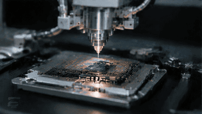
If there is one issue that links every advanced packaging technology in this roadmap, it is thermal management. 3D SoIC improves electrical proximity but worsens heat density. CPO reduces electrical loss but introduces thermal integration complexity around the optical engine and the adjacent ASIC. Chiplets improve architectural flexibility but can make the package more thermally uneven.
This means thermal capability will influence adoption order. Some 3D SoIC applications may move forward first because they are compact and high value enough to justify the cooling complexity. CPO may follow where the data movement problem is severe enough to justify optical integration. The roadmap is not linear because thermal realities are not linear.
Advanced packaging teams therefore need to think not only about what technology performs best electrically, but what technology can be cooled reliably at scale. That requirement often determines which roadmap stage is commercially viable first.
Packaging as an Ecosystem
Another big theme for 2027 is that advanced packaging can no longer be seen as a single process step or a single product type. It is an ecosystem. Foundries, OSATs, substrate makers, materials suppliers, equipment vendors, and test houses all have to align around the same integration goal. If one part of the chain lags, the roadmap slows down.
This ecosystem view matters because 3D SoIC and CPO have very different supply chain needs. SoIC depends heavily on precise bonding, thin-wafer handling, and yield control in stacked structures. CPO requires expertise in silicon photonics, optical alignment, laser coupling, and the integration of optical engines with high-speed ASICs. Both require advanced substrates, tight metrology, and strong test flows. But the exact capabilities are different, and the supply chain has to mature in parallel.
That is why the 2027 roadmap is as much about industrial readiness as it is about technology maturity. The winning platforms will be those that can move from lab demonstrations to repeatable manufacturing.
Where the Money Will Flow
The 2027 roadmap also hints at how capital will be allocated. Spending is likely to continue flowing into advanced packaging capacity, but not evenly. 3D SoIC will attract investment where vertical integration creates clear product differentiation. CPO will attract investment where optical bandwidth is the dominant constraint. Chiplet ecosystems will attract investment where modularity and reuse improve time to market and reduce risk.
This matters because advanced packaging has become a high-value part of the semiconductor stack. Companies are no longer investing only in wafer fabs. They are investing in package-level capability as a strategic asset. That is especially true in AI, where the package can determine whether the chip is competitive at all. In that environment, roadmap choices are also investment choices.
The companies that get the sequence right—vertical integration first where it matters, optical integration where it is needed, chiplet modularity throughout—will be the ones best positioned to capture value.
What 2027 May Look Like in Practice
By 2027, the packaging landscape will likely look more layered than revolutionary. That is not a bad thing. It means the technology stack is beginning to organize itself into practical tiers:
- 3D SoIC for dense, low-latency, vertically integrated local compute or memory structures.
- 2.5D and advanced fan-out for flexible chiplet assemblies and HBM integration.
- CPO for high-bandwidth, power-efficient system interconnect at the networking and infrastructure level.
This layered structure is probably the most realistic outcome. Not every product needs full 3D stacking. Not every system needs optics in the package. But many will need some combination of the three. The roadmap is therefore best understood as a portfolio of technologies, each positioned at a different point in the performance-cost-design space.
The Standards Question
No roadmap succeeds without standards. By 2027, the industry will need clearer interface expectations, better package design rules, and more robust test and qualification frameworks for both SoIC-style stacking and CPO systems. Standards matter because heterogeneous integration loses much of its value if every product requires a completely custom path.
For 3D SoIC, standards around die-to-die interfaces, bonding tolerances, and reliability qualification will be critical. For CPO, the need is even broader: optical engine interfaces, thermal assumptions, alignment strategies, and electrical-optical handoff rules all need to become more mature. The faster the industry can standardize the critical interfaces, the easier it will be to scale.
This is one reason 2027 feels like a roadmap year. The technology is maturing enough that common frameworks are becoming necessary. Without them, commercial adoption will remain fragmented.
What Designers Should Learn
For chip and system architects, the 2027 roadmap sends a clear message: packaging can no longer be treated as a downstream choice. It is part of architecture. Designers will need to think about:
- Whether vertical integration or optical interconnect solves the real bottleneck.
- How thermal constraints affect packaging selection.
- How chiplet partitioning changes the package and interconnect strategy.
- How the product roadmap may evolve from 3D SoIC-centric designs to optical-assisted systems.
That skill set will matter more every year. The best designs will likely be the ones that are package-aware from the start rather than adapted to packaging later.
Conclusion
The 2027 advanced packaging roadmap is really a story about convergence. 3D SoIC pushes vertical integration to its limits. CPO pushes electrical interconnect into the optical domain. Chiplets provide the modular structure that connects them. Together, they outline a future where the package is no longer just a container for the chip, but a platform for system design.
That future will not arrive all at once. It will unfold through a series of practical steps, with each technology finding its place where the economics and physics make sense. But the direction is clear. Advanced packaging and heterogeneous integration are moving from experimental differentiation to strategic infrastructure, and 2027 may be the year the roadmap becomes visible enough for everyone to follow.





